


RF board with SMPS
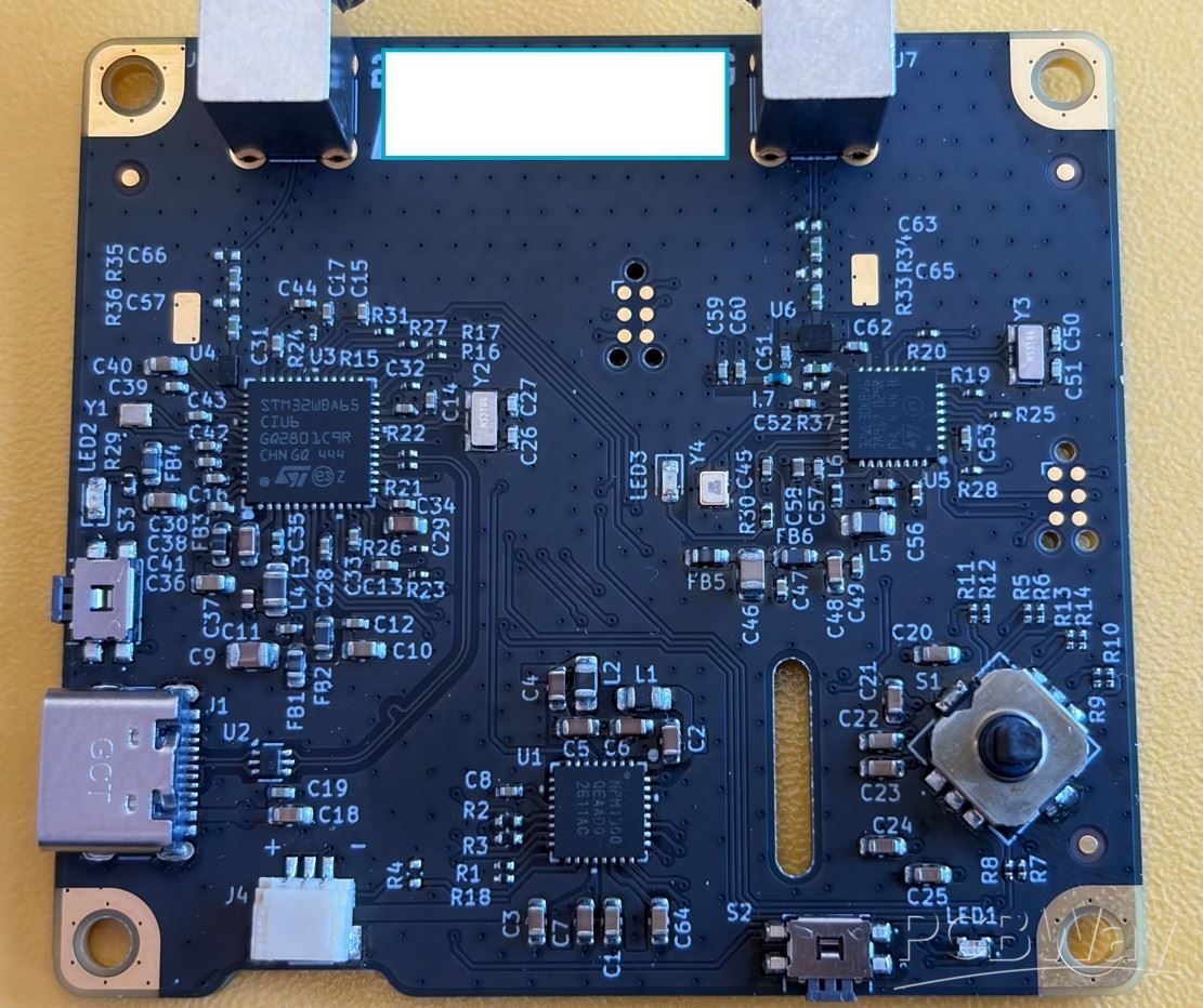
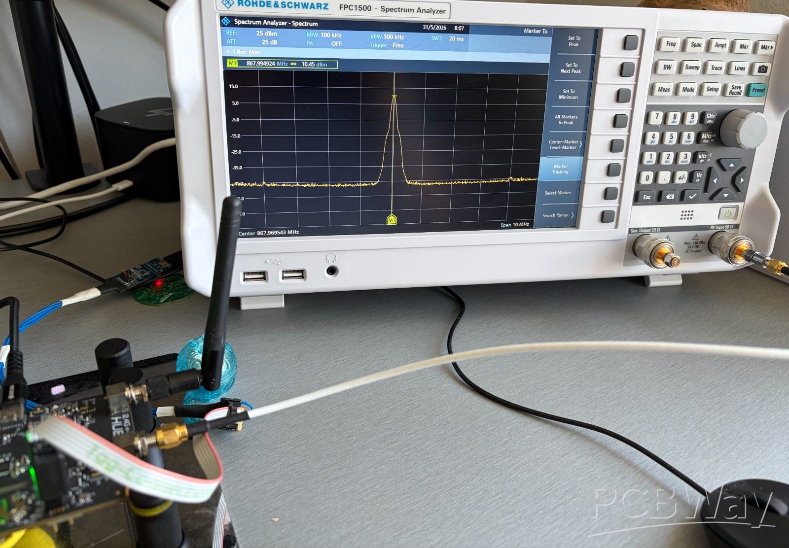
OUTSTANDING !!! Three controlled-impedance paths (USB 480 Mbit/s, RF1 at 2.5 GHz, and RF2) were successfully verified using both a VNA and a spectrum analyzer. Components such as QFN and BGA packages were soldered flawlessly, as confirmed by CT scan inspection. Small passive components in sizes ranging from 0201 to 0603 were also soldered perfectly—even without thermal relief, due to RF and SMPS constraints. The PCB features a custom stack-up, ENIG surface finish with through-hole plating, and 0.2 mm drill sizes. The black matte solder mask gives the board an excellent appearance. Overall, the build quality is perfect.
Jun 01,2026
20 viewsReport item
- Comments(0)
- Likes(0)
Upload photo
You can only upload 5 files in total. Each file cannot exceed 2MB. Supports JPG, JPEG, GIF, PNG, BMP
0 / 10000


